
Selecting the right transistor for your circuit design is a critical decision that directly impacts performance, reliability, and cost-effectiveness. Whether you're developing power supplies, audio amplifiers, switching circuits, or signal processing systems, the transistor you choose must align precisely with your electrical requirements, thermal constraints, and operational environment. This comprehensive guide walks you through the essential factors, technical parameters, and practical considerations that engineers and circuit designers must evaluate to make informed transistor selection decisions that ensure optimal circuit functionality and long-term reliability.
Understanding how to properly select a transistor requires analyzing multiple interdependent specifications including voltage ratings, current handling capacity, power dissipation limits, switching speed, gain characteristics, and package thermal properties. The wrong transistor choice can lead to circuit failure, thermal runaway, inadequate performance, or unnecessary cost overhead. This article provides a systematic approach to transistor selection, examining the key decision criteria across different circuit applications, helping you navigate the complex landscape of bipolar junction transistors, MOSFETs, and other semiconductor switch types to find the optimal component match for your specific engineering requirements.
Bipolar junction transistors represent one of the most widely used semiconductor devices in electronic circuits, functioning as both amplifiers and switches. A transistor of this type consists of three semiconductor layers forming either NPN or PNP configurations, where the current flow between collector and emitter is controlled by the base current. The current gain, typically denoted as beta or hFE, determines how much collector current flows for a given base current input, making these devices essential for signal amplification applications where small input signals must control larger output currents.
When selecting a bipolar transistor, engineers must consider the collector-emitter voltage rating, which defines the maximum voltage the device can withstand when fully off. Exceeding this voltage, even momentarily, can cause avalanche breakdown and permanent device damage. Similarly, the continuous collector current rating establishes the maximum sustained current the transistor can handle without thermal failure. For switching applications, bipolar transistors offer moderate switching speeds and require base drive current proportional to the load current, which influences driver circuit complexity and power consumption.
High-voltage bipolar transistors find extensive use in industrial power applications, particularly in switching power supplies, motor control circuits, and inductive load driving where robust voltage handling capabilities are essential. The selection process for these devices must account for safe operating area specifications, which define the simultaneous voltage and current conditions the transistor can safely handle during both steady-state and transient operations. Understanding these fundamental characteristics helps narrow down suitable transistor candidates based on your circuit's voltage, current, and gain requirements.
Metal-oxide-semiconductor field-effect transistors operate through voltage control rather than current control, offering distinct advantages in many circuit designs. A MOSFET transistor uses gate voltage to create a conductive channel between drain and source terminals, requiring virtually no continuous gate current once switched, which significantly reduces driver power requirements. This voltage-controlled operation makes MOSFETs particularly attractive for high-frequency switching applications, digital logic interfaces, and battery-powered systems where efficiency is paramount.
The selection criteria for MOSFET transistors center around drain-source voltage rating, continuous drain current capability, on-resistance, and gate charge characteristics. Low on-resistance minimizes conduction losses when the transistor is fully on, directly improving efficiency in power applications. Gate charge parameters determine how quickly the device can switch and how much energy the driver circuit must supply during each transition. For high-speed switching circuits, selecting a transistor with minimal gate charge and low input capacitance ensures fast switching transitions with reduced switching losses.
Power MOSFETs are available in both N-channel and P-channel variants, with N-channel devices offering better performance characteristics for equivalent die area. When designing circuits requiring bidirectional switching or high-side control, engineers must carefully evaluate whether P-channel transistors, despite their higher on-resistance, provide a simpler overall solution compared to N-channel devices with charge pump or bootstrap driver circuits. The transistor selection process must balance device-level performance against system-level complexity and cost considerations.
Beyond standard bipolar and MOSFET transistors, specialized devices address specific circuit challenges. Insulated-gate bipolar transistors combine MOSFET input characteristics with bipolar output characteristics, offering high voltage capability with relatively low on-state voltage drop. These hybrid devices excel in medium to high-power applications where the transistor must handle hundreds to thousands of volts while switching substantial currents efficiently.
Darlington transistors integrate two bipolar devices in a single package to provide very high current gain, simplifying driver circuits for high-current loads. However, the additional junction introduces higher saturation voltage, increasing conduction losses compared to single transistor implementations. Junction field-effect transistors operate with negative gate voltage relative to source, offering normally-on operation useful in specific circuit topologies. Understanding these specialized transistor categories expands your solution space when conventional devices cannot meet all design requirements simultaneously.
The transistor you ultimately select should represent the best compromise between electrical performance, thermal characteristics, availability, and cost for your particular application. Some circuits may benefit from newer wide-bandgap semiconductors like silicon carbide or gallium nitride transistors, which offer superior high-temperature performance and switching characteristics, albeit at higher component cost. Evaluating the full spectrum of available transistor technologies ensures your selection process considers all viable options rather than defaulting to familiar device types.
The absolute maximum voltage and current ratings form the foundation of transistor selection, defining the operational boundaries within which the device can safely function. For bipolar transistors, the collector-emitter breakdown voltage with base open establishes the maximum blocking voltage, while the collector-base breakdown voltage with emitter open may be higher but less relevant for typical circuit operation. Safety margins of at least twenty to fifty percent above normal operating voltages are standard practice to accommodate transient overvoltages from inductive switching, power supply variations, or external disturbances.
Current ratings include both continuous and pulsed specifications, with the latter allowing higher currents for brief durations based on thermal time constants. The transistor's continuous current rating assumes specific mounting and cooling conditions, typically 25 degrees Celsius ambient or case temperature. Real-world operating temperatures reduce usable current capacity, requiring derating curves provided in datasheets to determine actual safe current limits. Peak current ratings apply during switching transitions and must accommodate inrush currents when driving capacitive or initially discharged loads.
When driving inductive loads such as motors, solenoids, or transformers, the transistor must withstand voltage spikes that occur when current is interrupted. These inductive kickback voltages can reach several times the supply voltage, necessitating snubber circuits, clamping diodes, or selecting a transistor with sufficient voltage margin to survive these transients. The combination of current during conduction and voltage during blocking defines the power handling requirement that directly influences device cost and physical size.
Switching characteristics determine how quickly a transistor can transition between on and off states, directly impacting circuit performance in digital, switching power supply, and motor control applications. Rise time and fall time specifications indicate how fast the transistor voltage or current changes during transitions, while turn-on and turn-off delays account for internal charge storage and capacitive effects. For bipolar transistors, stored charge in the base region creates turn-off delays, with faster switching requiring forced base discharge through negative gate current or Baker clamps.
MOSFET switching speed depends primarily on gate charge and driver circuit capability. Total gate charge represents the electrical charge that must be supplied to transition the gate from one voltage state to another, directly determining switching energy losses. The transistor's input capacitance, output capacitance, and reverse transfer capacitance interact with circuit impedances to establish actual switching behavior. High-speed circuits require careful attention to gate drive circuit design, using low-impedance drivers and proper PCB layout to minimize parasitic inductance that can cause voltage ringing and electromagnetic interference.
Operating frequency affects transistor selection through switching losses, which increase proportionally with frequency. Each switching transition dissipates energy as the device passes through its active region where both voltage and current are simultaneously high. Higher frequency operation requires selecting a transistor with faster switching characteristics to minimize the time spent in this high-dissipation region. For converters operating above one hundred kilohertz, switching losses often exceed conduction losses, making fast-switching transistors with low gate charge more important than low on-resistance.
Current gain characteristics are crucial when selecting bipolar transistors for amplification or when optimizing driver circuit requirements. The DC current gain, typically specified as hFE or beta, varies with collector current, temperature, and individual device variation. Datasheets provide minimum gain values across operating conditions, but actual devices often exhibit higher gain. Insufficient gain margin forces driver circuits to supply excessive base current, increasing power consumption and potentially limiting switching speed through saturation effects.
For analog amplification applications, the transistor's small-signal parameters including transconductance, input impedance, and output impedance determine circuit gain, bandwidth, and linearity. Transistor selection must account for operating point stability over temperature, with gain variations potentially affecting bias conditions and performance. High-gain transistors minimize loading on previous stages and reduce component count in driver circuits, but may exhibit greater device-to-device variation requiring more sophisticated bias compensation techniques.
When using MOSFET transistors, transconductance indicates how effectively gate voltage changes control drain current in the active region, relevant for analog applications. However, most power electronics applications operate MOSFETs in fully-on or fully-off states, making threshold voltage and on-resistance more critical parameters than gain characteristics. The transistor selection process must prioritize specifications relevant to your specific circuit operating mode, whether amplification, linear regulation, or saturated switching.
Power dissipation within a transistor determines its thermal requirements and influences reliability, lifetime, and maximum safe operating current. Static power dissipation occurs when the transistor conducts current in its on-state, calculated as the product of on-state voltage drop and conducting current. For bipolar transistors, saturation voltage typically ranges from several hundred millivolts to over one volt depending on current level and device type. MOSFET on-resistance creates an I-squared-R loss that increases quadratically with current, making low on-resistance critical for high-current applications.
Dynamic power dissipation arises during switching transitions when the transistor passes through its active region with both significant voltage and current present simultaneously. This switching loss component increases with frequency and depends on switching speed, making it the dominant loss mechanism in high-frequency converters. The total power dissipation combines conduction losses, switching losses, and any gate drive losses, all of which must be removed through the device's thermal path to prevent junction temperature from exceeding maximum ratings, typically one hundred fifty to one hundred seventy-five degrees Celsius for silicon devices.
Calculating expected power dissipation requires analyzing both steady-state and transient operating conditions throughout your circuit's operating envelope. Worst-case scenarios typically occur at maximum load current, highest ambient temperature, and maximum input voltage conditions. The transistor you select must demonstrate adequate thermal margin under these conditions, accounting for additional derating in elevated ambient temperatures, high-altitude operation with reduced air density, or confined spaces with limited airflow. Thermal analysis early in the selection process prevents discovering thermal inadequacy after prototyping.
Thermal resistance characterizes how effectively heat flows from the transistor junction to the ambient environment, expressed in degrees Celsius per watt. The total thermal resistance comprises junction-to-case thermal resistance inherent to the transistor package, case-to-heatsink interface resistance affected by mounting technique and thermal interface material, and heatsink-to-ambient thermal resistance determined by heatsink geometry and airflow. These resistances sum serially, so the weakest thermal link dominates overall cooling effectiveness.
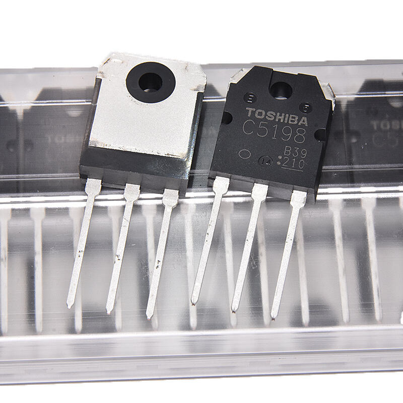
Package type significantly impacts thermal performance, with larger packages generally offering lower thermal resistance but consuming more board space. Through-hole packages like TO-220 and TO-247 provide mounting tabs that bolt directly to heatsinks for efficient heat extraction. Surface-mount packages such as DPAK, D2PAK, and various flat-pack configurations offer PCB-based cooling through copper pours and thermal vias, suitable for moderate power levels. The transistor package you choose must align with your board layout constraints, manufacturing processes, and thermal requirements.
Proper heatsink selection requires calculating the maximum allowable heatsink-to-ambient thermal resistance based on power dissipation, maximum ambient temperature, and maximum allowable junction temperature. Safety margins of ten to twenty degrees Celsius below maximum junction temperature improve reliability and account for thermal modeling uncertainties. Forced airflow dramatically improves heatsink effectiveness, allowing smaller heatsinks or higher power handling. When space constraints prevent adequate passive cooling, selecting a transistor with lower on-resistance reduces power dissipation, potentially eliminating heatsink requirements altogether.
When a single transistor cannot handle required current or power dissipation, parallel operation of multiple devices distributes the load. However, achieving equal current sharing between parallel transistors requires careful attention to device matching and circuit design. Bipolar transistors exhibit negative temperature coefficient of base-emitter voltage, meaning the device carrying slightly more current heats up, decreases its threshold voltage, and draws even more current in a runaway process. Preventing thermal runaway requires small source resistors, tight thermal coupling, or active current balancing circuits.
MOSFET transistors generally parallel more easily due to their positive temperature coefficient of on-resistance, which provides inherent current balancing. As one device carries more current, it heats up, increases its resistance, and naturally shifts current to cooler parallel devices. Despite this advantage, significant device mismatch or poor thermal coupling can still cause unequal current distribution. Selecting transistors from the same production batch minimizes parameter variation, while mounting all parallel devices on a common heatsink improves thermal coupling and promotes current sharing.
The decision to parallel multiple smaller transistors versus using one larger device involves trade-offs in cost, board space, thermal management, and circuit complexity. Multiple devices distribute heat generation more evenly but require more PCB area and component count. A single larger transistor simplifies circuit design but concentrates heat in one location and may cost more than multiple smaller devices. The optimal transistor selection considers system-level factors beyond individual device specifications, balancing electrical performance, thermal requirements, physical constraints, and overall cost.
The nature of your load significantly influences transistor selection requirements. Resistive loads present the simplest case, with steady current proportional to applied voltage and predictable power dissipation. Capacitive loads create high inrush currents during initial charging, requiring the transistor to handle peak current pulses that may far exceed steady-state values. Selecting a transistor with adequate pulsed current rating and considering series resistance to limit inrush ensures reliable operation without exceeding device safe operating area during transients.
Inductive loads such as motors, relays, solenoids, and transformers generate voltage spikes when current is interrupted, as stored magnetic energy converts to electrical energy seeking a current path. Without proper suppression, these voltage transients can exceed the transistor's voltage rating by several times, causing immediate failure. Protection strategies include flyback diodes across inductive loads, snubber networks combining resistors and capacitors, or selecting a transistor with sufficient voltage margin to absorb transients. The protection approach affects transistor selection by either requiring higher voltage rating or allowing use of lower-voltage devices with external protection.
Active loads that exhibit negative resistance characteristics or constant power behavior, such as electronic ballasts or motor controllers, can create stability challenges. The transistor and its drive circuit must maintain stable operation across the load's full impedance range, including startup transients and fault conditions. Understanding your load's electrical characteristics throughout all operating modes ensures the selected transistor specifications encompass worst-case demands rather than just nominal operating conditions, preventing field failures from unanticipated load behavior.
The transistor's drive requirements must match available control signals and driver capabilities. Bipolar transistors require base current proportional to collector current divided by current gain, with insufficient base current preventing full saturation and increasing conduction losses. High-current applications may necessitate driver transistors or integrated gate drivers to supply adequate base current from logic-level control signals. When selecting a transistor, consider whether your control circuit can supply necessary drive current or whether additional driver stages add unacceptable complexity and cost.
MOSFET drive circuits must supply sufficient current to charge the gate capacitance within the required switching time, with faster switching demanding higher peak gate current. Logic-level MOSFETs operate with gate voltages compatible with three-volt or five-volt logic, while standard MOSFETs may require ten to fifteen volts for full enhancement. The transistor selection must account for available gate drive voltage, with logic-level devices simplifying interface circuitry but typically offering higher on-resistance for equivalent die area. Dedicated gate driver integrated circuits provide the high peak currents necessary for fast switching while isolating low-power control circuits from high-power transistor switching.
Level-shifting requirements arise when controlling high-side transistors or when control circuits operate at different voltages than power circuits. Bootstrap circuits, charge pumps, or isolated gate drivers enable MOSFET control with gate voltage referenced to source rather than ground. Alternatively, selecting P-channel MOSFETs for high-side switching or using bipolar transistors that operate with ground-referenced base signals may simplify driver design despite device performance trade-offs. The transistor selection process must consider the complete driver circuit chain, balancing device performance against system complexity and reliability requirements.
The safe operating area graphically represents simultaneous voltage and current conditions the transistor can sustain without damage or degradation. SOA curves typically show several boundaries including maximum continuous current, maximum power dissipation hyperbola, maximum voltage, and secondary breakdown limits. During switching transitions, the transistor temporarily operates in its active region with high voltage and current simultaneously present. The trajectory through voltage-current space during switching must remain within SOA boundaries, with pulse duration limits becoming more restrictive for longer pulses as thermal mass saturates.
Designing with appropriate margins above nominal conditions accounts for component tolerances, environmental variations, aging effects, and unexpected transients. Conservative design practice maintains at least twenty percent margin on voltage ratings, fifteen percent margin on current ratings, and fifty percent margin on power dissipation under worst-case conditions. These margins may seem excessive during benchtop testing at room temperature with carefully selected components, but prove essential for reliable field operation across production variations, temperature extremes, and extended service life.
Reliability considerations extend beyond absolute maximum ratings to include stress factors affecting long-term degradation. Operating junction temperature strongly influences failure rates, with each ten-degree increase approximately doubling semiconductor failure probability according to Arrhenius models. Voltage stress, even within ratings, accelerates degradation mechanisms. Frequent thermal cycling creates thermomechanical stress at material interfaces. The transistor selection process should favor devices with ratings substantially above operating requirements, allowing cooler operation that dramatically improves reliability and extends operational lifetime, particularly in critical applications where field failures impose significant consequences.
The most critical specification depends on your specific application requirements, but voltage rating, current capacity, and power dissipation form the essential triad for power transistor selection. Your transistor must handle the maximum voltage present when off, carry required current when on, and dissipate resulting power losses within thermal limits. Overlooking any of these three primary specifications will lead to device failure, so they must be evaluated together with appropriate safety margins. For high-frequency switching applications, switching speed and gate charge become equally important as they determine switching losses that may exceed conduction losses.
Bipolar transistors generally excel in applications requiring high voltage capability with moderate switching speeds, such as linear amplifiers, low-frequency switching, and circuits where current gain reduces driver complexity. MOSFETs are preferred for high-frequency switching, high-efficiency power conversion, and applications where the voltage-controlled input simplifies driver design and reduces power consumption. If your circuit operates above fifty kilohertz, requires minimal driver power, or needs very low conduction losses at moderate voltages, MOSFETs typically provide better performance. For high-voltage industrial applications above six hundred volts, bipolar or IGBT transistors may offer advantages in cost and ruggedness.
Using a transistor with higher voltage and current ratings than required is generally acceptable and often improves reliability through increased safety margins. However, higher-rated devices typically have higher input capacitance, gate charge, or lower current gain, which may affect switching speed or driver requirements. Ensure the substitute transistor's package and pinout match your PCB layout and that thermal characteristics remain compatible with your cooling solution. Electrical parameters like threshold voltage, on-resistance, and saturation voltage should be similar to maintain circuit performance. Always verify critical timing and loss calculations with actual substitute device parameters rather than assuming complete interchangeability based solely on maximum ratings.
Package type directly affects thermal performance, board mounting method, power handling capability, and circuit layout. Through-hole packages like TO-220 provide excellent thermal performance with heatsink mounting but require more board space and complicate automated assembly. Surface-mount packages enable higher assembly density and automated manufacturing but typically offer higher thermal resistance, limiting power dissipation unless extensive copper thermal planes are used. The transistor package must align with your manufacturing process, available board space, power dissipation requirements, and thermal management strategy. Some packages provide multiple pins connected to the same terminal to reduce lead inductance and improve current handling, important for high-frequency or high-current applications.