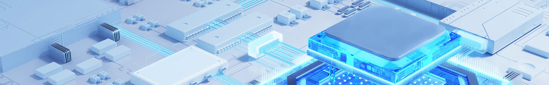
Surface Mount Technology (SMT) has dramatically transformed printed circuit board assembly by enabling smaller components and higher-density layouts. SMT involves positioning components directly on the surface of the PCB, bypassing the need for traditional through-hole assembly methods. This advancement facilitates compact and intricate designs, contributing significantly to enhanced electrical performance. High-speed placement machines further amplify these benefits, allowing for substantial throughput increases and reduced labor costs. According to industry data, SMT implementation can improve production speeds by over 50%, while its precision reduces defect rates significantly. This innovation is a cornerstone of PCB assembly automation, driving efficiency across consumer electronics, automotive, and medical device sectors.
Touchless manufacturing lines represent a cutting-edge approach to PCB assembly automation, significantly reducing human error. This method integrates robotics and machine vision systems to automate the entire production process—from component placement to inspection—without physical human intervention. Notably, Absolute EMS Inc., a leader in electronics manufacturing, showcases such an approach by employing optical inspection stations seamlessly within their manufacturing workflow (Absolute EMS Inc., 2024). This technology enhances quality control, as evidenced by studies showing a 30% reduction in assembly defects compared to traditional processes. Robotics and machine vision systems embedded in touchless lines ensure meticulous quality checks at each stage, setting a new standard in PCB assembly efficiency and reliability.
New Product Introduction (NPI) is crucial in the PCB manufacturing landscape, as it streamlines the journey from concept to market-ready products. Modern process preparation software significantly enhances NPI by optimizing the entire manufacturing process. This software plays an instrumental role in improving workflow efficiency, reducing production errors, and decreasing time-to-market timelines. For instance, it can automate the transition from PCB design to manufacturing, ensuring that every detail aligns with production capabilities. Successful implementations of NPI optimization software have shown notable improvements, such as reducing production lead times by up to 50%. This not only accelerates innovation but also allows PCB manufacturers to meet the rising demand for printed circuit board assembly in today's competitive market.
The role of 3D inspection systems in PCB assembly is pivotal for achieving precision quality control. These systems elevate the quality control process by providing a more detailed analysis than traditional 2D inspections. They are adept at detecting subtle defects and anomalies that might be overlooked with conventional inspection methods, such as solder joint irregularities or component misalignments. For example, advancements in 3D vision technology have allowed for real-time inspection, resulting in defect reduction rates of up to 70%. By identifying potential faults early, PCB manufacturers can ensure higher quality products, reduce rework costs, and enhance customer satisfaction, which is crucial in maintaining a competitive edge in the market.
Hybrid soldering techniques, which blend traditional methods with advanced technologies, have revolutionized PCB manufacturing by optimizing outcomes. These processes incorporate various techniques like laser soldering and selective soldering, offering flexibility and precision that are essential for modern PCB designs. Material innovations play a significant role in these processes by improving the resilience and reliability of solder joints. For instance, the development of advanced solder alloys enhances joint durability, thereby extending the lifecycle of the PCB. These improvements in materials and methods have proven effective, with case studies showing up to a 50% increase in joint reliability. Hybrid soldering, therefore, not only bolsters the integrity of the printed circuit board assembly but also propels PCB manufacturers towards more sustainable and efficient production practices.
Managing component density in PCB design presents several challenges which require innovative strategies for effective circuit integration. High-density designs often risk signal interference and overheating, demanding meticulous layout planning to minimize these issues. Integrated circuit integration furthers the complexity, influencing how designs are structured to maintain performance. As PCBs evolve, integrating increasingly intricate circuits is essential. Successful examples, such as high-count BGAs within sophisticated PCBs, demonstrate that utilizing efficient routing techniques can significantly enhance design outcomes. Techniques such as micro vias and impedance control are pivotal in achieving these complex configurations, ensuring the circuit's stability and performance.
Effective thermal management is crucial in maintaining PCB performance, especially in complex configurations. Without proper heat dissipation strategies, overheating could compromise functionality and lifespan. Implementing thermal management techniques like copper-filled vias, heat sinks, or thermal pads can substantially mitigate these risks. Studies indicate that robust thermal management significantly extends PCBs’ longevity, underlining its importance in the design process. By adhering to best practices in thermal mitigation, designers achieve a balance between high density and optimal temperature control, ensuring the reliability and efficiency of the assembled PCBs even under demanding conditions.
When selecting a PCB manufacturer, assessing technical capabilities is crucial. The key capabilities to consider include the types of equipment used, such as advanced printed circuit board assembly machines, precision drilling technologies, and automated inspection systems. These technologies ensure the production of high-quality PCBs and the reliability of the final product. Additionally, certifications like ISO 9001 and IPC standards are essential indicators of the manufacturer's commitment to quality and industry norms. Here's a checklist to help evaluate potential PCB manufacturers:
These steps will help ensure that you select a manufacturer who can meet the demands of both current and future PCB production needs.
AS9100 compliance is a standardized quality management system crucial for manufacturers in the aerospace sector, reflecting a commitment to reliability and safety. This standard helps ensure products meet stringent aerospace quality requirements. For PCB manufacturers, achieving AS9100 compliance signifies their capability to produce highly precise and reliable printed circuit boards, critical in aerospace applications. Balancing cost efficiency while maintaining compliance involves adopting streamlined processes, such as automated PCB design and printed circuit board assembly technologies. It's also beneficial to engage industry experts for insights on best practices. Strategies can include:
By applying these strategies, businesses can effectively manage costs while ensuring their PCB manufacturers meet AS9100 compliance, thus maintaining product quality and reliability.
Southeast Asia has established itself as a powerhouse in electronics manufacturing by leveraging logistical and economic advantages. The region boasts a strategic geographic location that facilitates seamless trade routes, reducing transportation costs and delivery times significantly. Additionally, Southeast Asia's favorable economic conditions, such as competitive labor costs and rich resource availability, further bolster its manufacturing appeal. In recent years, countries like Vietnam, Malaysia, and Thailand have emerged as key leaders, contributing significantly to the region's manufacturing shift. According to recent data, Southeast Asia's supply chain performance metric surpasses many global counterparts, reinforcing its pivotal role in the electronics industry.
The rapid implementation of 5G networks and the widespread adoption of the Internet of Things (IoT) are major catalysts propelling the growth of PCB and electronics manufacturing in the Asia-Pacific region. 5G technology is revolutionizing the industry by providing faster and more reliable connectivity, which is crucial for high-density electronic components manufacturing. IoT, on the other hand, is augmenting demand and driving innovation as more devices are interconnected, necessitating advanced integrated circuits and printed circuit boards. Industry forecasts suggest a continued upsurge in the market, with 5G and IoT technologies expected to drive substantial growth, creating new opportunities for PCB manufacturers and designers to innovate and thrive in the evolving electronics landscape.