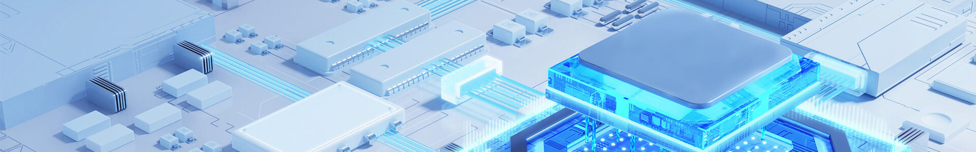
AI-driven automation plays a crucial role in precision manufacturing within the PCB assembly industry. By adopting artificial intelligence, manufacturers have streamlined their processes, significantly reducing errors and enhancing the speed of assembly. Companies leveraging AI technologies in PCB assembly have reported substantial productivity improvements. According to industry statistics, the adoption of AI has resulted in a productivity increase of up to 30% in some cases, showcasing its profound impact on operational efficiency.
Real-world examples further illustrate the efficacy of AI-driven automation. Leading PCB manufacturers have harnessed AI to optimize assembly lines, leading to faster production cycles and a reduction in component defects. This integration not only minimizes human intervention but also ensures that precision standards are consistently met. By embracing AI technologies, these manufacturers are setting a benchmark in the industry, paving the way for future advancements in precision PCB assembly.
High-Density Interconnect (HDI) technology is pivotal for modern circuit boards, especially in high-frequency applications. HDI allows more components to be packed into smaller areas, enhancing the functionality of devices like smartphones and tablets. One effective strategy for implementing HDI in PCB design involves specific layering techniques, such as microvias and blind or buried vias, which cater to the increasing demand for compactness.
Incorporating a mix of innovative materials, such as low-loss laminates, also helps meet the exigencies of modern device specifications. Industry experts suggest that the future of HDI in PCB assembly will witness further advancements and challenges, including the need for even higher precision and reliability as electronics continue to shrink in size. These insights underscore the importance of evolving strategies to stay ahead in the ever-changing landscape of PCB design.
As components on PCBs become smaller and more intricate, advanced soldering techniques are essential to keep up with these trends. Techniques such as selective soldering and laser soldering have become increasingly important. Selective soldering allows for precise application of solder to specific areas, while laser soldering offers high precision for delicate components.
Thermal management is vital during the soldering process of miniaturized components to maintain functionality and avoid damage. Proper thermal management ensures that components operate efficiently without overheating, which is crucial for maintaining the reliability and efficiency of PCBs. For instance, incorporating these soldering methods can significantly increase the reliability of connections and extend the lifespan of assembled products. These advancements in soldering techniques are crucial for meeting the high demands of modern electronic devices in terms of performance and durability.
High-frequency substrates play a crucial role in elevating the performance of 5G and IoT devices. These substrates typically include materials such as ceramics and composites that aid in improved signal integrity and reduced loss. A study highlighted in the Journal of Electronics suggests that modern materials used in these substrates can significantly minimize signal distortion and enhance device performance. The consistent development in substrate technology is noteworthy, with trends leaning towards the utilization of newer materials like low-loss dielectric substrates expected to further elevate the capabilities of these high-frequency applications.
Flexible PCBs are ideally suited for wearable technology due to their unique properties like bendability and lightweight design. Recent innovations include the use of polyimide and hybrid materials, which allow for enhanced flexibility and durability. Polyimide materials are particularly instrumental as they can withstand rigorous use better than traditional PCBs, enabling a myriad of applications in consumer electronics. Market trends indicate a growing demand for flexible PCBs as manufacturers explore new possibilities to satisfy consumer desire for more versatile and compact electronic devices.
In the quest for sustainability, the environmental impact of traditional PCB materials necessitates a shift towards biodegradable alternatives. Traditionally, PCBs have relied heavily on non-renewable materials which are not environmentally friendly. Emerging biodegradable materials such as polylactic acid and cellulose-based composites are pioneering eco-friendly PCB manufacturing. Research published in the Journal of Sustainable Electronics has confirmed the effectiveness and reliability of these materials, showcasing their potential to transform PCB manufacturing into a more sustainable industry. Using eco-friendly materials not only minimizes waste but also aligns with growing consumer preferences for greener products.
Sustainable manufacturing practices are becoming increasingly important, with PCB manufacturers adopting energy-efficient methodologies to reduce overhead costs and environmental impact. Several strategies include upgrading machinery to more energy-efficient models, conducting detailed energy audits, and optimizing production processes. These initiatives result in quantifiable reductions in both energy consumption and operational costs, significantly benefiting the manufacturers. By adopting sustainability initiatives, companies not only achieve financial savings but also enhance their brand reputation, reflecting a commitment to environmental responsibility.
PCB waste disposal presents numerous challenges, necessitating robust recycling protocols within PCB assembly services. The growing mountain of electronic waste underscores the urgent need for effective recycling systems. Statistics reveal a worldwide increase in electronic waste, emphasizing the importance of sustainability practices in the industry. Leading companies in the PCB sector are implementing innovative initiatives to promote recycling. These programs aim to minimize waste and repurpose components effectively, showcasing the industry's dedication to environmental stewardship.
The shift to lead-free soldering within PCB assembly is crucial for regulatory compliance and addressing environmental concerns. Lead-free soldering techniques have been developed to mitigate the harmful effects of lead, which traditionally served as a primary component in soldering processes. Implementing these techniques effectively involves using suitable materials, ensuring compatibility without compromising performance. While the transition to lead-free methods poses challenges, data indicates that PCB manufacturers are steadily adopting these practices. The emphasis is on overcoming obstacles to ensure compliance and promote sustainability within PCB assembly services, benefiting both the environment and the industry at large.
Advancements in PCB circuitry for electric vehicles are revolutionizing power management and efficiency systems. As the demand for electric vehicles grows, manufacturers have focused on developing PCBs that enhance power delivery, manage battery performance, and optimize energy usage. Industry statistics reflect significant growth in EV markets, correlating to increasing PCB demand. For instance, the compound annual growth rate for electric vehicles is expected to rise by 23% between 2023 and 2032, necessitating more advanced automotive PCBs. Companies like PCBWay are pioneering innovations in this area, crafting PCBs designed specifically for the demanding requirements of EV power management, heralding a new era of automotive electronics.
Aerospace-grade PCBs are engineered to withstand extreme conditions, ensuring reliability and durability. These requirements include resilience to high temperatures, vibration, and pressure variance, vital for equipment used in aerospace applications. To achieve such durability, PCB manufacturers often utilize materials like polyimide and techniques such as thermal management systems. Case studies, such as those involving Boeing's reliance on robust PCBs, demonstrate the critical role these circuit boards play in successful aerospace endeavors. These circuits ensure system integrity and reliability in space missions and aircraft developments, fortifying the industry's trust in specialized PCB solutions.
Medical device PCBs demand exceptional reliability due to their critical role in patient safety and performance. Enhancements in this field focus on sustaining device accuracy and operational longevity. Technologies such as biocompatible materials and advanced assembly processes are employed to fortify PCB reliability. Successful integrations are seen in devices like pacemakers and MRI machines, which rely on these advanced PCB designs for superior functionality. Leading manufacturers, including Benchmark Electronics, have implemented stringent reliability enhancements to support the evolving needs of medical technology, ensuring patient trust and safety remain paramount in healthcare solutions involving electronic devices.
3D printing technologies have made significant strides in circuit board prototyping, offering unparalleled speed and customization. These advancements allow for rapid fabrication processes that drastically reduce the time needed to develop PCB prototypes, effectively modernizing supply chains traditionally reliant on lengthy manufacturing cycles. As a result, companies can iterate designs faster, leading to more innovative and tailored products. Notable for their contributions in this area are [Nano Dimension](https://www.nano-di.com/) and [BotFactory](https://botfactory.co/), pioneers in developing 3D-printed circuit boards. These organizations are reshaping the PCB industry by integrating advanced printing techniques that enhance the versatility and scalability of circuit board production.
The dawn of quantum computing necessitates a rethink of PCB architectures to accommodate unique demands. Quantum computing harnesses quantum bits and requires PCBs designed with specialized materials and configurations to support unique processing capabilities. Active research explores hybrid materials and innovative designs optimized for quantum applications, ensuring compatibility with these sophisticated systems. A promising future market is anticipated as quantum technologies reach real-world applications in sectors like computing, data security, and complex problem-solving. PCBs customized for quantum computing represent a frontier in circuit board design innovation, promising to redefine possibilities within technological sectors.
Photonics is crucial in revolutionizing PCB design by significantly boosting communication and processing speeds. By integrating photonic elements into circuit designs, the transmission of data becomes nearly instantaneous, and signal integrity is vastly improved, paving the way for future high-demand applications. Solutions that incorporate photonics are gaining traction, with innovators like [Intel](https://www.intel.com) championing these technologies to enable rapid data transfer and enhance overall device functionality. Forecast growth in photonic-infused PCBs promises a transformative impact across industries, leveraging light waves for highly efficient data processing and unlocking new technological possibilities. As photonic integration in PCB design spreads, sectors such as telecommunications, computing, and aerospace stand to benefit greatly from these advancements.