High-Density PCBAs represent a revolutionary advancement in electronics manufacturing, enabling engineers to pack more functionality into smaller form factors than ever before. These sophisticated printed circuit board assemblies utilize advanced design techniques and cutting-edge components to achieve unprecedented levels of miniaturization while maintaining optimal performance. As electronic devices continue to shrink in size while expanding in capability, High-Density PCBAs have become the backbone of modern technology across industries ranging from consumer electronics to aerospace applications.
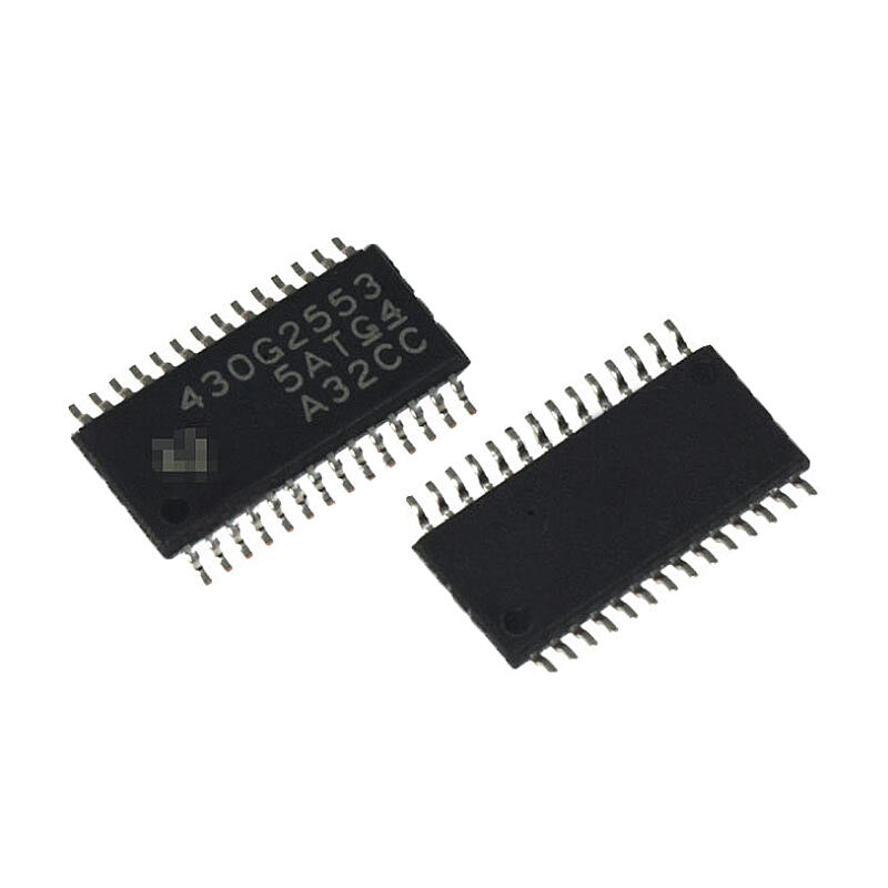
The fundamental architecture of High-Density PCBAs involves the strategic placement of components using advanced mounting techniques that maximize board real estate efficiency. These assemblies typically incorporate Ball Grid Array packages, Quad Flat No-lead components, and other surface-mount technologies that allow for extremely tight component spacing. The substrate materials used in High-Density PCBAs often feature multiple layers with microvias and buried vias, enabling complex routing patterns that would be impossible with traditional PCB designs.
Modern High-Density PCBAs leverage advanced materials science to achieve superior electrical performance while maintaining mechanical reliability. The dielectric materials used in these assemblies must exhibit excellent thermal stability, low loss characteristics, and dimensional stability across varying environmental conditions. Additionally, the copper trace geometries in High-Density PCBAs are precisely controlled to minimize signal integrity issues and electromagnetic interference that could compromise system performance.
Manufacturing High-Density PCBAs requires exceptional precision and adherence to stringent quality standards throughout the production process. Advanced placement equipment capable of positioning components with sub-micron accuracy is essential for achieving the tight tolerances required in high-density designs. The soldering processes used for these assemblies often involve specialized techniques such as selective soldering, vapor phase reflow, and nitrogen atmosphere processing to ensure reliable joint formation.
Quality assurance for High-Density PCBAs involves comprehensive testing protocols that verify both electrical functionality and mechanical integrity. Automated optical inspection systems examine solder joint quality, component placement accuracy, and potential defects that could impact long-term reliability. In-circuit testing and functional testing ensure that each assembly meets specified performance criteria before shipment to customers.
One of the most significant advantages of High-Density PCBAs is their ability to maximize functionality within severely constrained space requirements. Modern electronic devices demand increasingly complex functionality while consumers expect smaller, more portable products. High-Density PCBAs address this challenge by enabling designers to integrate multiple subsystems onto a single compact board, eliminating the need for separate modules and reducing overall system volume.
The space optimization achieved through High-Density PCBAs extends beyond simple component placement strategies. These assemblies often incorporate three-dimensional design approaches, utilizing both sides of the PCB substrate and implementing stacked component configurations where appropriate. This multi-dimensional approach allows engineers to achieve component densities that would be impossible with traditional single-sided or simple double-sided designs.
High-Density PCBAs contribute significantly to weight reduction in electronic systems, a critical consideration in applications such as portable devices, automotive electronics, and aerospace systems. By consolidating multiple functions onto fewer boards and utilizing smaller component packages, these assemblies reduce both the total material volume and the associated weight of interconnecting hardware such as connectors, cables, and mechanical support structures.
The material efficiency achieved through High-Density PCBAs also translates to reduced manufacturing costs and environmental impact. Smaller boards require less substrate material, fewer processing chemicals, and reduced packaging materials for shipping and handling. This efficiency becomes particularly important in high-volume manufacturing scenarios where even small material savings can result in significant cost reductions over the product lifecycle.
High-Density PCBAs offer superior electrical performance characteristics compared to traditional board designs, primarily due to reduced signal path lengths and optimized component placement. The compact nature of these assemblies minimizes parasitic capacitances and inductances that can degrade signal quality, particularly at high frequencies. Shorter interconnection paths also reduce signal propagation delays, enabling faster system operation and improved timing margins.
The advanced layer stack-up configurations used in High-Density PCBAs provide excellent power distribution and ground plane integrity, essential for maintaining clean power supplies to sensitive analog and digital circuits. These designs often incorporate dedicated power and ground planes with strategic placement of decoupling capacitors to minimize power supply noise and voltage fluctuations that could impact circuit performance.
Effective thermal management is crucial for High-Density PCBAs due to the concentrated heat generation resulting from closely packed components. Advanced thermal design techniques such as thermal vias, heat spreading layers, and strategic component placement help distribute heat more effectively across the board substrate. Some high-performance applications may also incorporate embedded heat sinks or thermal interface materials to enhance heat dissipation capabilities.
The reliability of High-Density PCBAs benefits from reduced interconnection complexity and fewer mechanical joints that could potentially fail over time. By consolidating functionality onto fewer boards, these assemblies eliminate many traditional failure points such as board-to-board connectors, cable assemblies, and mechanical mounting hardware. This consolidation approach often results in improved overall system reliability and reduced maintenance requirements.
High-Density PCBAs offer significant cost advantages in high-volume production scenarios through improved manufacturing efficiency and reduced assembly complexity. The consolidation of multiple functions onto fewer boards reduces the total number of assemblies that must be manufactured, tested, and handled during production. This simplification of the manufacturing process translates to reduced labor costs, shorter production cycle times, and improved overall manufacturing yield rates.
The economies of scale achieved through High-Density PCBAs become particularly apparent when considering the total cost of ownership for electronic systems. While the initial design and setup costs for these advanced assemblies may be higher than traditional approaches, the long-term savings in manufacturing, assembly, and testing often provide substantial return on investment for medium to high-volume applications.
High-Density PCBAs simplify supply chain management by reducing the total number of unique assemblies and components that must be procured, tracked, and managed throughout the production process. This consolidation reduces inventory carrying costs, minimizes the risk of component shortages affecting multiple assembly lines, and simplifies quality control procedures across the manufacturing operation.
The standardization opportunities enabled by High-Density PCBAs allow manufacturers to develop common platform designs that can be adapted for multiple product variants through software configuration or minor component changes. This platform approach further reduces development costs, shortens time-to-market for new products, and enables more efficient utilization of manufacturing resources across product lines.
The consumer electronics industry has been one of the primary drivers for High-Density PCBAs development, with smartphones, tablets, and wearable devices demanding ever-increasing functionality in progressively smaller form factors. These applications require High-Density PCBAs that can accommodate complex processing capabilities, wireless communication modules, sensor arrays, and power management systems within space-constrained enclosures.
Wearable technology represents an extreme example of the space optimization benefits provided by High-Density PCBAs. Smartwatches, fitness trackers, and medical monitoring devices must integrate sophisticated electronics into form factors that are comfortable for extended wear while maintaining battery life and performance expectations. The miniaturization enabled by High-Density PCBAs has made these applications commercially viable and continues to drive innovation in wearable technology.
Modern automotive electronics increasingly rely on High-Density PCBAs to integrate the complex control systems required for advanced driver assistance systems, infotainment platforms, and vehicle electrification. These applications demand assemblies that can operate reliably in harsh environmental conditions while providing the computational power necessary for real-time system control and data processing.
Industrial automation and Internet of Things applications benefit from the ruggedization capabilities that can be incorporated into High-Density PCBAs designs. These assemblies can be optimized for specific environmental requirements such as temperature extremes, vibration resistance, and chemical exposure while maintaining the compact form factors necessary for integration into existing industrial equipment and machinery.
Successful High-Density PCBAs design requires careful consideration of component selection and placement strategies that optimize both electrical performance and manufacturing feasibility. Component selection must balance electrical specifications, package size, thermal characteristics, and availability to achieve the desired functionality within the available board real estate. Advanced design tools enable engineers to evaluate multiple placement scenarios and optimize routing efficiency before committing to final layouts.
The placement strategy for High-Density PCBAs must consider thermal interactions between components, signal routing requirements, and accessibility for testing and rework procedures. Critical analog circuits may require isolation from digital switching circuits to prevent interference, while high-power components must be positioned to facilitate effective heat dissipation without affecting temperature-sensitive components.
Testing and validation of High-Density PCBAs requires specialized techniques and equipment capable of accessing closely spaced test points and verifying functionality in space-constrained configurations. Boundary scan testing, in-circuit testing, and functional testing strategies must be incorporated into the design from the earliest stages to ensure adequate test coverage without compromising the density advantages of the final assembly.
Validation methodologies for High-Density PCBAs often involve accelerated life testing and environmental stress screening to verify long-term reliability in the intended application environment. These testing protocols help identify potential failure modes and validate design margins before full-scale production, reducing the risk of field failures and warranty costs.
The future development of High-Density PCBAs will be driven by advances in substrate materials and manufacturing processes that enable even greater miniaturization and performance improvements. Flexible and rigid-flex substrates are becoming increasingly important for applications requiring three-dimensional assembly configurations or integration into curved or irregularly shaped enclosures.
Emerging substrate technologies such as glass-based PCBs and ceramic substrates offer superior electrical properties and thermal performance compared to traditional organic materials. These advanced substrates enable High-Density PCBAs designs with finer trace geometries, higher layer counts, and improved signal integrity characteristics that will be essential for next-generation high-frequency applications.
The integration of High-Density PCBAs with emerging technologies such as artificial intelligence processors, 5G communication systems, and advanced sensor technologies will drive continued innovation in assembly design and manufacturing techniques. These applications will require High-Density PCBAs capable of supporting extremely high data rates, complex signal processing requirements, and sophisticated power management capabilities.
System-in-Package and chip-scale packaging technologies will further enhance the capabilities of High-Density PCBAs by enabling the integration of multiple semiconductor die within single component packages. This approach allows for even greater functionality consolidation and can reduce the total component count required for complex electronic systems.
High-Density PCBAs offer several key advantages including significant space savings, improved electrical performance through shorter signal paths, reduced system weight, enhanced reliability through fewer interconnections, and cost efficiency in high-volume production. These assemblies enable greater functionality integration while maintaining or improving overall system performance compared to traditional multi-board approaches.
While High-Density PCBAs may have higher initial design and setup costs, they typically provide significant cost savings in medium to high-volume production through reduced assembly complexity, fewer components to manage, and simplified testing procedures. Production timelines can be shortened due to fewer separate assemblies requiring manufacturing and integration, though initial design and validation phases may require additional time investment.
High-Density PCBAs must be designed with careful attention to thermal management due to concentrated heat generation from closely packed components. Environmental considerations include vibration resistance, temperature cycling capability, and protection from moisture and contaminants. Reliability is generally improved through reduced interconnection complexity, but requires careful component selection and validation testing to ensure long-term performance in the intended application environment.
Industries that benefit most from High-Density PCBAs include consumer electronics, automotive, aerospace, medical devices, telecommunications, and industrial automation. These sectors typically require compact, lightweight solutions with high functionality density and reliable operation in challenging environments. The specific benefits vary by application but generally include space savings, weight reduction, improved performance, and cost efficiency.