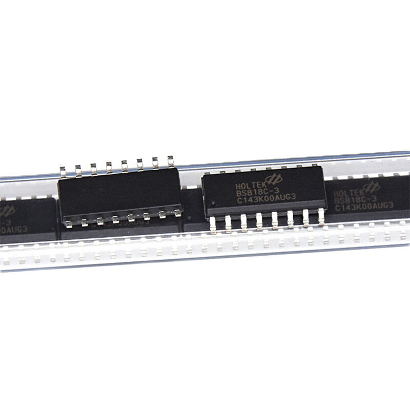
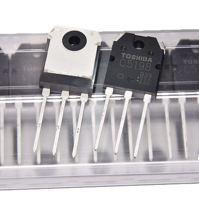
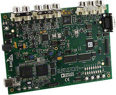
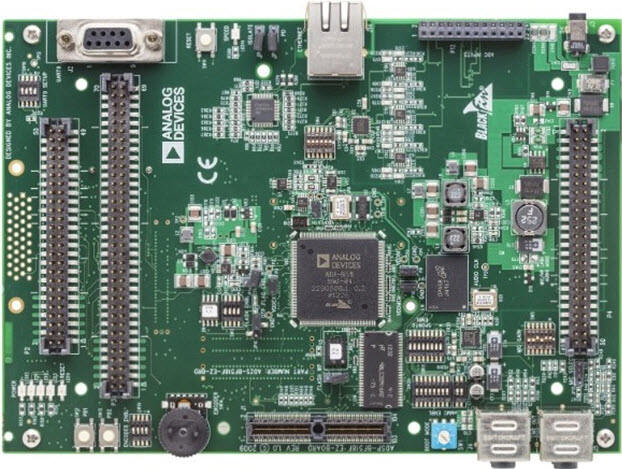
صفحه ی PCB دوطرفه
یک برد مدار چاپی دوطرفه نشاندهنده پیشرفت قابل توجهی در طراحی مدارهای الکترونیکی است و از لایههای مسی هادی در هر دو سطح بالا و پایین زیرلایه تشکیل شده است. این پیکربندی امکان طراحی مدارهای پیچیدهتر و تراکم قطعات بیشتر را نسبت به برندهای تکطرفه فراهم میکند. ساختار این برد معمولاً شامل یک ماده هستهای، معمولاً FR4، با لایههای مسی که به هر دو طرف آن متصل شدهاند، میشود که این لایهها از طریق سوراخهای فلزی (plated through holes) یا ویاس ها به هم متصل میشوند. این اتصالات بینلایهای اجازه میدهند سیگنالهای الکتریکی بین دو طرف برد عبور کنند و امکان مسیریابی کارآمدتر و عملکرد بهبودیافتهتری ایجاد شود. برد مدار چاپی دوطرفه امروزه در الکترونیک مدرن ضروری شده است و در کاربردهای متنوعی از جمله الکترونیک مصرفی تا سیستمهای اتوماسیون صنعتی مورد استفاده قرار میگیرد. این برد دارای یکپارچگی بهتر سیگنال، محافظت الکترومغناطیسی بهبودیافته و استفاده کارآمدتر از فضا است. فرآیند تولید آن شامل تکنیکهای دقیق لایهگذاری، سوراخکاری، روکشدهی و اچ کردن است تا اتصالات قابل اعتمادی بین قطعات ایجاد شود. این بردها قادر به نصب قطعات SMD و قطعات سوراخدار (through hole) در هر دو طرف خود هستند که این امر انعطافپذیری طراحی و تراکم مدار را به حداکثر میرساند. وجود صفحات زمین (ground planes) در هر یک از طرفها نیز به عملکرد الکتریکی بهتر و کاهش تداخل الکترومغناطیسی کمک میکند.