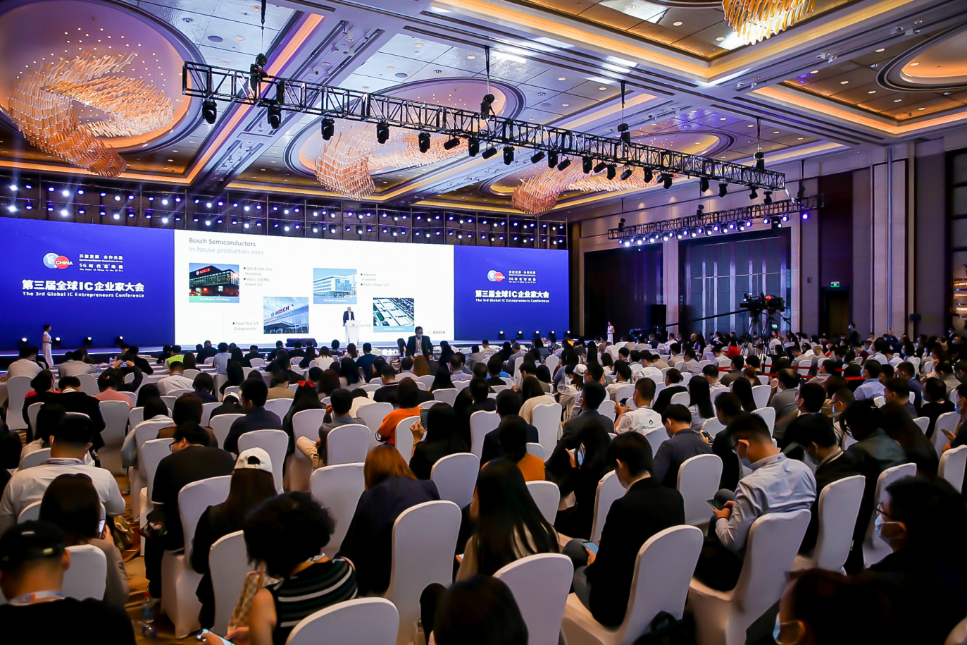
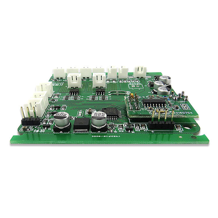
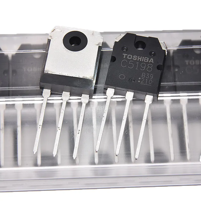
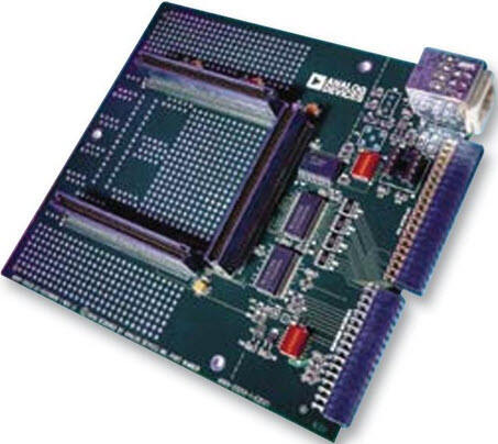
conception et fabrication de PCB
La conception et la fabrication de cartes électroniques constituent le pilier fondamental de la fabrication moderne de l'électronique, englobant un processus sophistiqué qui transforme des concepts électroniques en cartes de circuits tangibles. Ce processus complet implique la création de schémas détaillés, de dispositions des composants et de configurations multicouches qui forment la base des dispositifs électroniques. La phase de conception utilise des logiciels CAO avancés pour positionner précisément les composants, établir les connexions électriques et optimiser l'intégrité du signal. Lors de la fabrication, les fabricants utilisent des techniques de pointe telles que la photolithographie, la gravure et l'assemblage automatisé pour produire des cartes de circuits de haute qualité. Ce processus s'adapte à diverses spécifications, allant des cartes simples monocouches à des conceptions complexes multicouches intégrant des interconnexions haute densité. La conception et la fabrication modernes de cartes électroniques prennent en compte des éléments essentiels tels que la gestion thermique, la compatibilité électromagnétique et l'analyse de l'intégrité du signal. Ces cartes servent de colonne vertébrale à d'innombrables applications, allant de l'électronique grand public et des systèmes automobiles aux dispositifs médicaux et au matériel aérospatial. Le secteur évolue constamment avec les technologies émergentes, en intégrant des matériaux avancés et des méthodes de fabrication afin de répondre aux exigences croissantes en matière de miniaturisation et d'amélioration des performances.