design e fabricação de pcb
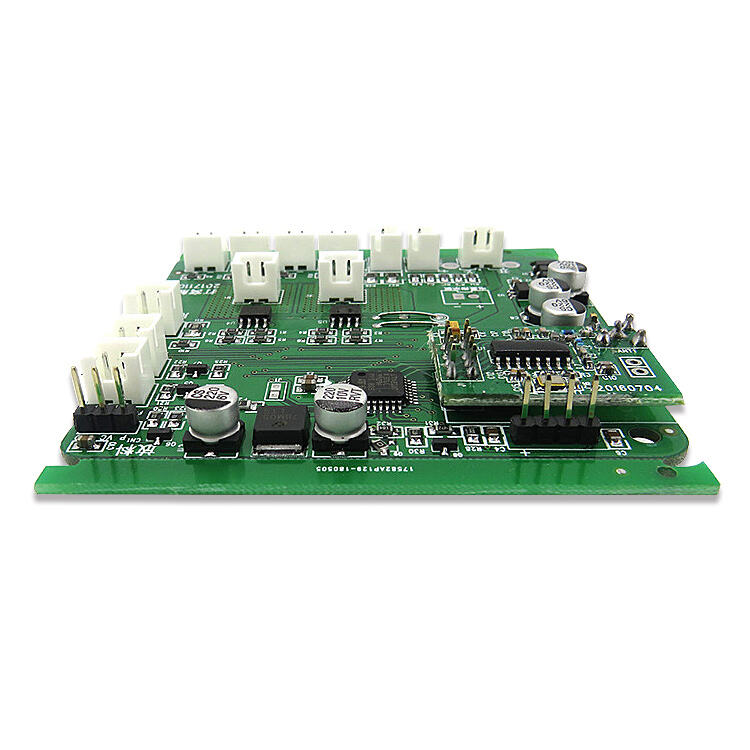
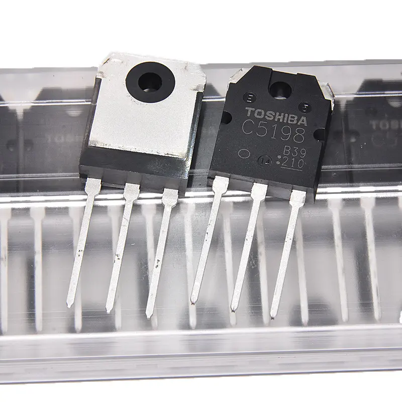
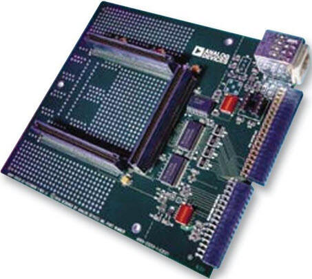
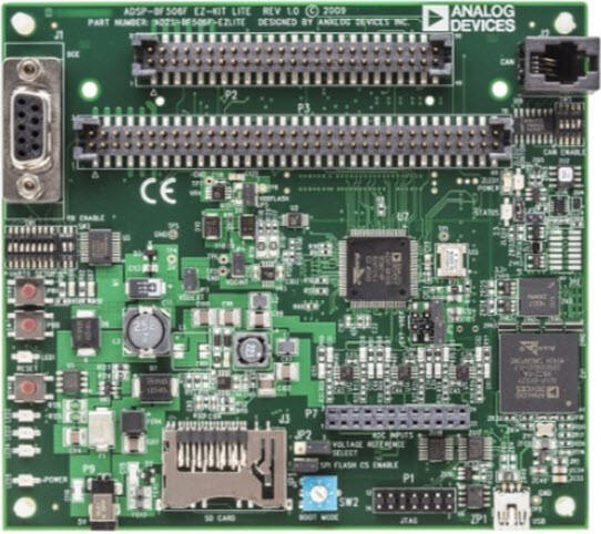
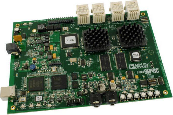
O projeto e a fabricação de PCBs representam a pedra angular da moderna indústria de eletrônicos, englobando um processo sofisticado que transforma conceitos eletrônicos em placas de circuito concretas. Esse processo abrangente envolve a criação de esquemáticos detalhados, layouts de componentes e configurações com múltiplas camadas que formam a base dos dispositivos eletrônicos. A fase de projeto utiliza softwares avançados de CAD para posicionar com precisão os componentes, estabelecer conexões elétricas e otimizar a integridade dos sinais. Durante a fabricação, os fabricantes empregam técnicas de última geração, incluindo fotolitografia, gravação química e montagem automatizada, para produzir placas de circuito de alta qualidade. O processo acomoda diversas especificações, desde placas simples de uma única camada até projetos complexos multicamadas com interconexões de alta densidade. O projeto e a fabricação modernos de PCBs incorporam considerações essenciais, como gerenciamento térmico, compatibilidade eletromagnética e análise de integridade de sinal. Essas placas servem como estrutura fundamental para inúmeras aplicações, que vão desde eletrônicos de consumo e sistemas automotivos até dispositivos médicos e equipamentos aeroespaciais. A indústria evolui constantemente com tecnologias emergentes, implementando materiais avançados e métodos de fabricação para atender à crescente demanda por miniaturização e melhoria de desempenho.