
As IoT ecosystems continue to expand across industries—from smart agriculture and industrial monitoring to wearable health devices and connected home systems—the power management challenge has become one of the most critical engineering decisions designers face. A PMIC, or Power Management Integrated Circuit, sits at the heart of every efficient IoT design, coordinating voltage regulation, battery charging, load switching, and power sequencing within a compact footprint. Choosing the right PMIC is not merely a component selection exercise; it directly shapes the device's battery life, thermal performance, reliability, and overall system cost.
Understanding what features define an ideal PMIC for IoT devices requires looking beyond datasheet headline numbers. IoT applications impose a unique set of demands: ultra-low quiescent current for always-on sensing, wide input voltage tolerance to handle variable energy sources, high integration density to minimize board space, and robust noise rejection to protect sensitive RF and analog circuitry. This article systematically breaks down the key attributes that distinguish a purpose-fit PMIC from a generic power management solution, helping engineers and procurement professionals make better-informed decisions for their connected device designs.
In a conventional industrial power supply design, quiescent current of a few hundred microamps is rarely a concern. In IoT, however, a device may spend 99% of its operational life in a deep sleep state, waking briefly to sample a sensor or transmit a data packet. During these extended sleep intervals, the PMIC itself must consume the absolute minimum current to avoid draining the battery prematurely. A PMIC with a quiescent current in the single-digit microamp range can extend battery life from months to years, fundamentally changing the economics and serviceability of a deployed IoT node.
The quiescent current specification refers to the current drawn by the PMIC internally to maintain its own regulation loops, bias circuits, and reference voltages, even when no load is connected. In IoT scenarios where coin cells, thin-film batteries, or harvested energy sources are used, this parasitic consumption is a dominant factor in total energy budget calculations. Engineers targeting multi-year battery life must treat the PMIC's sleep-mode current as a first-tier selection criterion rather than an afterthought.
Modern IoT-optimized PMIC designs achieve this through innovative bandgap reference trimming, adaptive bias current circuits, and selective power-gating of internal blocks. The result is a regulator that can maintain output regulation at microamp-level load currents without instability or dropout—a capability that generic PMICs often cannot provide.
While sleep-mode efficiency captures the most attention, an IoT PMIC must also transition rapidly and cleanly from sleep to active mode. Many IoT microcontrollers and radio transceivers impose strict power-on sequencing requirements, and the PMIC must deliver stable supply rails within microseconds of a wake event. Slow transient response can cause brown-out resets, corrupt data transactions, or failed radio link establishment—all of which degrade system reliability and increase average current consumption through repeated retry cycles.
A well-designed PMIC for IoT will specify transient load response alongside its static quiescent current, demonstrating that it can handle the abrupt current spike when a processor transitions from sleep to full compute load without the output voltage collapsing below the minimum operating threshold. This dynamic behavior is often more revealing of real-world suitability than steady-state efficiency curves alone.
IoT devices are deployed in environments where the power source may be anything from a stable USB connection to a deteriorating primary cell, a solar harvesting circuit with fluctuating panel output, or an RF energy harvesting front-end with millivolt-level inputs. An ideal PMIC must tolerate a wide input voltage range to remain functional and protect downstream electronics across these varied and often unpredictable supply conditions.
Wide input range capability in a PMIC is not simply about supporting high voltages—it equally concerns the ability to operate down to very low input voltages near the battery's discharge endpoint. A PMIC that loses regulation or enters an undefined state as battery voltage droops below 2.0V is unsuitable for any IoT design where maximum energy extraction from the source is a priority. Low dropout voltage specifications directly determine how much usable capacity is extracted from every battery cell.
Energy harvesting compatibility adds another dimension. Photovoltaic, thermoelectric, and piezoelectric sources produce raw power that fluctuates in both voltage and current. An IoT-suitable PMIC may incorporate maximum power point tracking, input under-voltage lockout with hysteresis, and cold-start mechanisms that allow the system to initialize from extremely low harvested voltages. These features collectively enable truly batteryless or battery-assisted IoT nodes that can operate indefinitely in the field without human intervention.
Industrial and outdoor IoT deployments expose power inputs to electrostatic discharge, inductive load kickback, and conducted transients from shared power rails. A robust PMIC design incorporates integrated input protection structures, reverse polarity protection, and overvoltage clamping to prevent damage during installation or operation in harsh environments. These protections reduce the need for discrete external components, simplifying the bill of materials and improving overall system reliability.
The combination of wide input range and integrated protection makes a well-specified PMIC the cornerstone of a fault-tolerant power architecture. For IoT devices deployed in locations where maintenance is costly or infrequent, this resilience directly translates into lower total cost of ownership and higher uptime guarantees for the end application.
Board space in IoT devices is an uncompromising constraint. Whether the design is a wearable patch, a miniaturized asset tracker, or a sensor node embedded in infrastructure, every square millimeter of PCB area is precious. A highly integrated PMIC that combines multiple power rails, charging management, load switches, and supervisory functions within a single IC dramatically reduces the component count compared to discrete implementations using separate LDOs, DC-DC converters, and charge controllers.
This integration benefit extends beyond board area. Fewer discrete components mean fewer solder joints, reduced assembly complexity, simplified procurement, and lower probability of component-level failures. For high-volume IoT products where manufacturing yield and supply chain simplicity drive profitability, a well-integrated PMIC can be a decisive competitive advantage. The design investment required to qualify and characterize a single PMIC is far less than validating a cluster of five or six independent power management components.
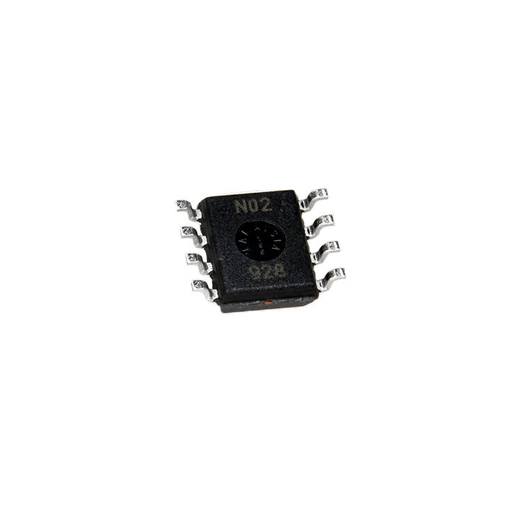
Package form factor matters equally. Compact packages such as SOIC-8, DFN, WLCSP, and QFN allow dense placement near the load they supply, minimizing parasitic inductance and resistance on critical power traces. A PMIC available in a thermally efficient small package, like the SOIC-8 configuration used by solutions such as the PMIC variants optimized for low-noise LDO regulation, enables tighter layout and better signal integrity throughout the power distribution network.
Modern IoT SoCs, RF transceivers, and sensor arrays typically require multiple supply voltages—a core logic rail, an I/O voltage rail, an analog reference voltage, and sometimes a dedicated RF supply. A PMIC that delivers all of these from a single device with programmable sequencing logic eliminates the risk of voltage rail contention and ensures that sensitive circuits power up and power down in the correct order every time.
Proper power sequencing enforced by the PMIC prevents latch-up conditions in CMOS logic, protects ESD structures that can be damaged when I/O pins receive voltage before the core supply is established, and satisfies the initialization requirements specified in SoC datasheets. For IoT devices that undergo frequent sleep-wake cycling, this sequencing reliability is exercised thousands of times over the product lifetime, making it a non-negotiable feature of any serious PMIC selection.
IoT devices almost universally include wireless communication subsystems—Bluetooth Low Energy, Zigbee, LoRa, NB-IoT, or Wi-Fi. These radio front-ends are acutely sensitive to power supply noise, particularly at frequencies that alias into the RF signal chain or that modulate the local oscillator frequency. A PMIC that generates high switching noise can degrade receiver sensitivity, increase transmit error rates, and cause regulatory compliance failures in radiated emission testing.
LDO-type PMIC stages are inherently favored for RF supply because they produce lower output noise than switching regulators. However, even LDO designs differ significantly in their output noise spectral density, particularly in the 10 Hz to 100 kHz range where many communication protocols are sensitive. A PMIC with a specified output noise density below 30 µV RMS in this band provides meaningful protection for co-located radio hardware, reducing the need for bulky external filtering.
Beyond radio coexistence, low supply noise benefits analog sensing circuits—ADC front-ends, pressure transducers, optical detectors, and electrochemical sensors all exhibit noise floors that are partly determined by power supply quality. An IoT PMIC that delivers clean, quiet supply rails directly improves measurement resolution and sensor data quality, which are ultimately what give the connected device its application value.
Power Supply Rejection Ratio, or PSRR, quantifies how effectively a PMIC's output attenuates noise present at the input. A high PSRR across a broad frequency range means that even when the battery voltage experiences switching artifacts from other system components, the regulated output delivered to sensitive loads remains clean and stable. For IoT designs where a single battery powers both switching converters and precision analog circuits simultaneously, PSRR is an essential discriminator when evaluating competing PMIC options.
Engineers should evaluate PSRR not just at 1 kHz, where most datasheets publish a favorable single-point figure, but across the entire frequency range relevant to their system. A PMIC with 70 dB PSRR at 1 kHz but only 20 dB at 100 kHz provides far less protection than one that sustains high rejection through the MHz range. This frequency-dependent behavior significantly affects how much external decoupling capacitance is needed to achieve acceptable noise performance in the final design.
Small IoT devices have limited thermal mass and almost no forced airflow, meaning any power dissipated inside the enclosure raises junction temperatures quickly. A PMIC operating at high dropout voltage while supplying peak load currents during radio transmission bursts can become a localized heat source that degrades surrounding components and accelerates electromigration in PCB copper traces. Selecting a PMIC with appropriate junction-to-ambient thermal resistance for the package and use case is therefore a reliability-critical decision.
Thermal protection features integrated within the PMIC—such as over-temperature shutdown and thermal foldback current limiting—serve as the last line of defense when ambient conditions exceed design assumptions or when a fault condition causes unexpected power dissipation. These protections prevent permanent damage and allow graceful recovery rather than catastrophic failure, which is particularly important in IoT deployments where physical access for repair is limited or expensive.
IoT infrastructure is often expected to operate continuously for five to ten years or more without maintenance. A PMIC selected for these applications must demonstrate long-term reliability through AEC-Q100 qualification or equivalent accelerated life testing. Mean time between failures, electromigration limits, and humidity-bias performance are all relevant data points for infrastructure-grade IoT deployments in outdoor, industrial, or medical environments.
Procurement and design engineers should also consider supply chain longevity when selecting a PMIC. A component scheduled for end-of-life within three years creates significant redesign risk for a product with a ten-year intended field life. Sourcing from distributors with confirmed long-horizon inventory and working with suppliers who provide product longevity guarantees reduces the total lifecycle risk of the chosen PMIC solution.
Ultra-low quiescent current is the most critical feature for battery-powered IoT devices because the device spends the majority of its time in sleep mode. A PMIC that draws only a few microamps in standby can extend battery life from months to years. Alongside quiescent current, low dropout voltage ensures maximum energy is extracted from the battery as it discharges, making both specifications essential for maximizing operational life between replacements or recharging cycles.
Yes, highly integrated PMIC solutions are specifically designed to provide multiple regulated output rails from a single device, covering core logic, I/O, analog reference, and RF supply voltages. These multi-rail PMIC devices also incorporate power sequencing logic to ensure each rail powers up and shuts down in the correct order as required by the SoC manufacturer. The degree of integration available depends on the specific device family, so engineers must match the PMIC's output rail count and sequencing flexibility to their SoC's power architecture requirements.
Wireless transceivers used in IoT devices are extremely sensitive to power supply noise because voltage fluctuations on the supply rail modulate the RF signal chain, degrading receiver sensitivity and transmit signal quality. A PMIC with high output noise can cause increased bit error rates, reduced communication range, and failed regulatory compliance in radiated emission testing. Selecting a PMIC with low output noise spectral density and high PSRR across the relevant frequency range ensures that the radio subsystem operates at its specified performance level without requiring extensive external filtering.
Package type directly affects thermal resistance, parasitic inductance, PCB footprint, and placement flexibility. A PMIC in a compact package such as SOIC-8 or WLCSP can be placed very close to the load it supplies, minimizing parasitic resistance and inductance on the power trace, which improves transient response and reduces conducted noise. Thermal resistance varies significantly between packages, so engineers must verify that the chosen PMIC package can dissipate the expected power under worst-case ambient and load conditions without exceeding the device's maximum junction temperature rating.