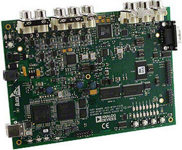
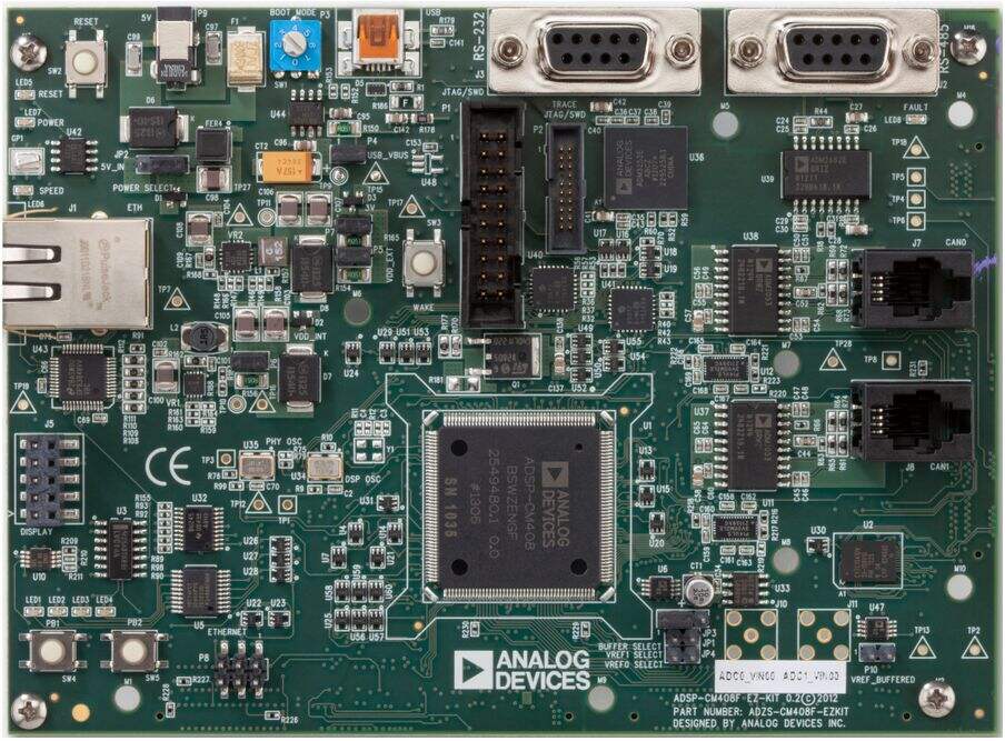
High Frequency PCB: Advanced Signal Integrity Solutions for Premium RF Applications

high frequency pcb

High frequency PCBs (Printed Circuit Boards) represent a sophisticated advancement in electronic circuit manufacturing, specifically designed to handle signals operating at frequencies typically above 1 GHz. These specialized boards are engineered with precise impedance control, minimal signal loss, and superior electromagnetic compatibility. The construction involves carefully selected materials with specific dielectric constants and loss tangents, such as Rogers, Taconic, or PTFE-based substrates, which maintain signal integrity at high frequencies. The design incorporates specific layout techniques including controlled trace widths, precise spacing, and ground plane optimization to manage electromagnetic interference and maintain signal quality. High frequency PCBs are essential in modern telecommunications equipment, radar systems, satellite communications, and high-speed digital devices. They feature specialized copper foil treatments, precise thickness controls, and advanced surface finishes to ensure optimal performance. The manufacturing process demands extreme precision in drilling, etching, and lamination to maintain the critical electrical characteristics required for high-frequency applications. These boards often include additional design elements such as striplines, microstrip transmission lines, and carefully calculated vias to maintain signal integrity throughout the circuit path.

Popular Products

High frequency PCBs offer numerous compelling advantages that make them indispensable in modern electronic applications. First, they provide superior signal integrity at high frequencies, ensuring minimal signal distortion and loss during transmission. This results in cleaner, more reliable communications and data transfer. The specialized materials used in these boards offer excellent thermal stability, preventing performance degradation under varying temperature conditions. These PCBs demonstrate exceptional electromagnetic interference (EMI) resistance, crucial for maintaining signal quality in complex electronic systems. The precise impedance control achieved through careful design and manufacturing helps minimize signal reflection and maximize power transfer. Their low signal loss characteristics enable longer transmission distances without significant degradation. High frequency PCBs also offer excellent dimensional stability, ensuring consistent performance over time and environmental changes. The specialized surface treatments and finishes provide superior conductivity and reduced skin effect at high frequencies. These boards support higher component density while maintaining signal quality, allowing for more compact design solutions. Their reliability in demanding applications reduces system maintenance requirements and extends operational life. The controlled dielectric properties ensure predictable performance across the entire frequency range of operation. Additionally, these PCBs offer better power handling capabilities at high frequencies compared to standard boards, making them ideal for high-power RF applications.

Tips And Tricks

China International Semiconductor Expo

11

Sep

China International Semiconductor Expo

Join Jeking at China International Semiconductor Expo, showcasing cutting-edge ICs, diodes, and semiconductor solutions for the global market.
View More
The Impact Of Integrated Circuits On Consumer Electronics

12

Sep

The Impact Of Integrated Circuits On Consumer Electronics

Integrated circuits have revolutionized consumer electronics by enabling miniaturization, enhancing performance, reducing costs, and expanding device functionality.
View More
Understanding Soldering Techniques in PCBA

15

Oct

Understanding Soldering Techniques in PCBA

Master the art of soldering in PCBA with Jeking's comprehensive guide to techniques and high-quality components.
View More
Market Demand and Future of OEM PCBA

16

Dec

Market Demand and Future of OEM PCBA

The OEM PCBA market experiences robust demand, driven by the expanding electronics industry and the need for customized, efficient manufacturing solutions.
View More

Get a Free Quote

Our representative will contact you soon.
Email
Name
Company Name
Message
0/1000

high frequency pcb

Advanced Material Technology

Advanced Material Technology

High frequency PCBs utilize cutting-edge material technology that sets them apart from conventional circuit boards. The core materials, typically including specialized laminates like Rogers, Taconic, or advanced PTFE composites, are specifically engineered to maintain stable dielectric properties across a wide frequency range. These materials exhibit remarkably low loss tangents, typically less than 0.002, ensuring minimal signal attenuation even at frequencies exceeding 10 GHz. The carefully controlled dielectric constant (Dk) remains stable across temperature variations, preventing impedance fluctuations that could compromise signal integrity. The copper foil used in these boards undergoes special treatment processes to achieve ultra-smooth surfaces, reducing signal losses due to skin effect at high frequencies. This material excellence translates to superior performance in demanding applications where signal precision is paramount.
Precision Manufacturing Process

Precision Manufacturing Process

The manufacturing process for high frequency PCBs represents the pinnacle of precision electronics fabrication. Each step is meticulously controlled to maintain critical tolerances that directly impact electrical performance. The etching process employs advanced techniques to achieve exact trace geometries, with width tolerances often held to within ±0.001 inches. Layer-to-layer registration is maintained with exceptional accuracy, typically within 0.002 inches, ensuring proper alignment of transmission lines and vias. The drilling process utilizes specialized equipment capable of producing micro-vias with precise depth control and minimal drill wandering. The lamination process is carefully controlled for temperature and pressure to maintain material stability and prevent delamination issues that could affect electrical performance.
Superior Signal Integrity Solutions

Superior Signal Integrity Solutions

The signal integrity capabilities of high frequency PCBs demonstrate their exceptional value in modern electronic systems. These boards incorporate sophisticated design elements specifically engineered to maintain signal quality at high frequencies. The controlled impedance transmission lines are designed and manufactured to tight tolerances, typically maintaining ±10% or better impedance control across the entire board. Ground plane designs include specific features to minimize return path inductance and reduce common-mode noise. The strategic placement of vias and ground connections helps maintain consistent impedance transitions between layers. Advanced electromagnetic simulation tools are used during the design phase to optimize signal paths and minimize crosstalk between adjacent traces. This comprehensive approach to signal integrity results in superior performance in high-speed digital and RF applications.

Get a Free Quote

Our representative will contact you soon.
Email
Name
Company Name
Message
0/1000
Attachment
Up to 3 files,more 30mb,suppor jpg、jpeg、png、pdf、doc、docx、xls、xlsx、csv、txt、stp、step、igs、x_t、dxf、prt、sldprt、sat、rar、zip