पीसीबी डिजाइन और निर्माण
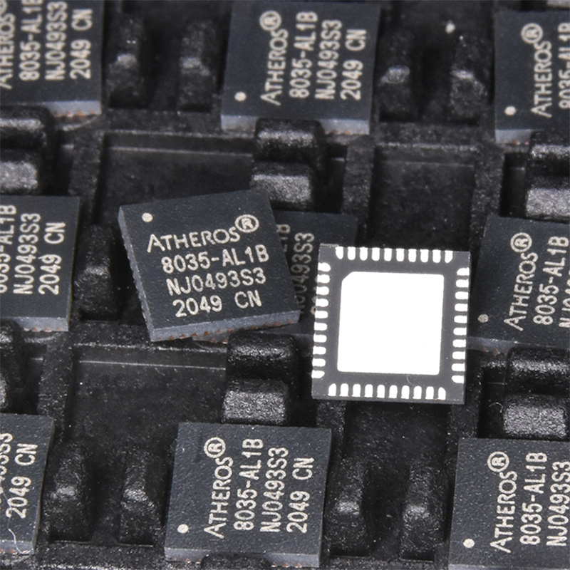
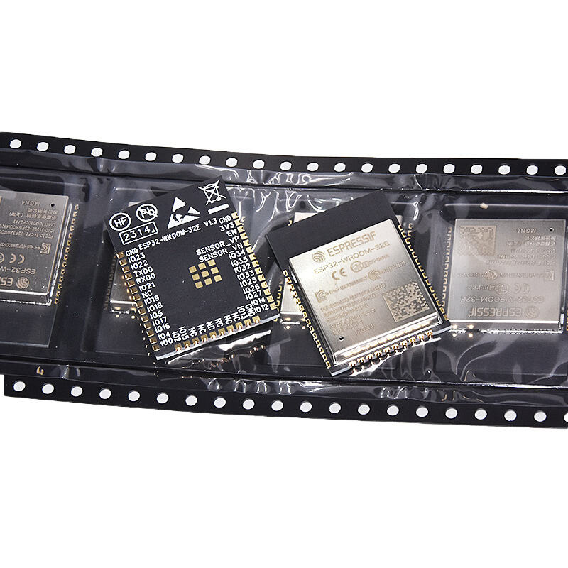
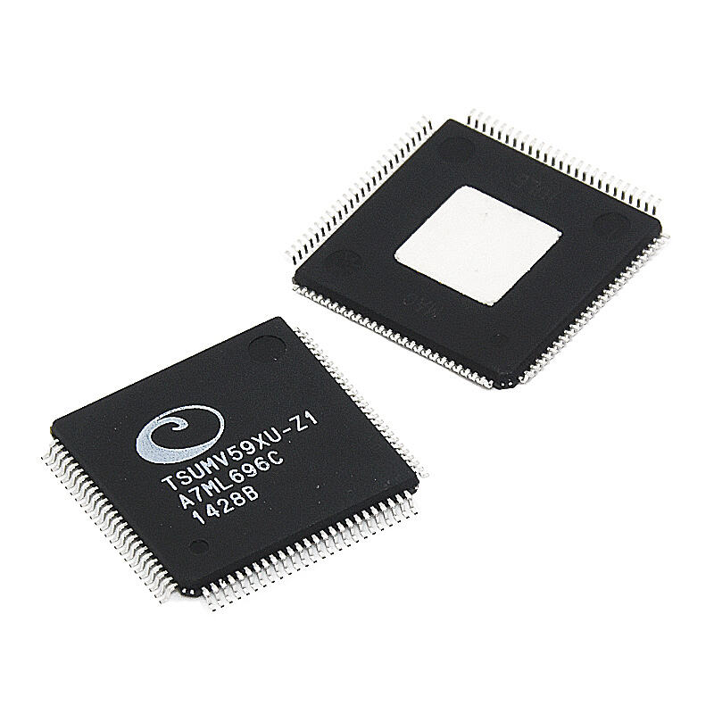
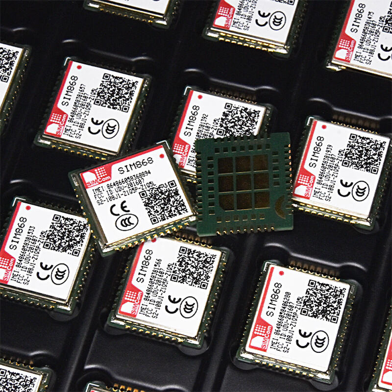
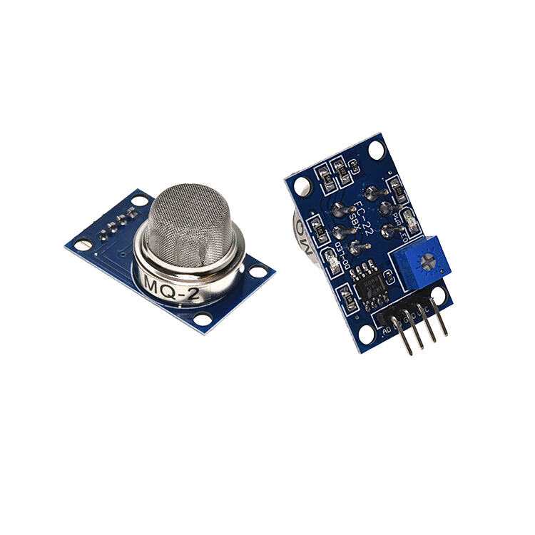
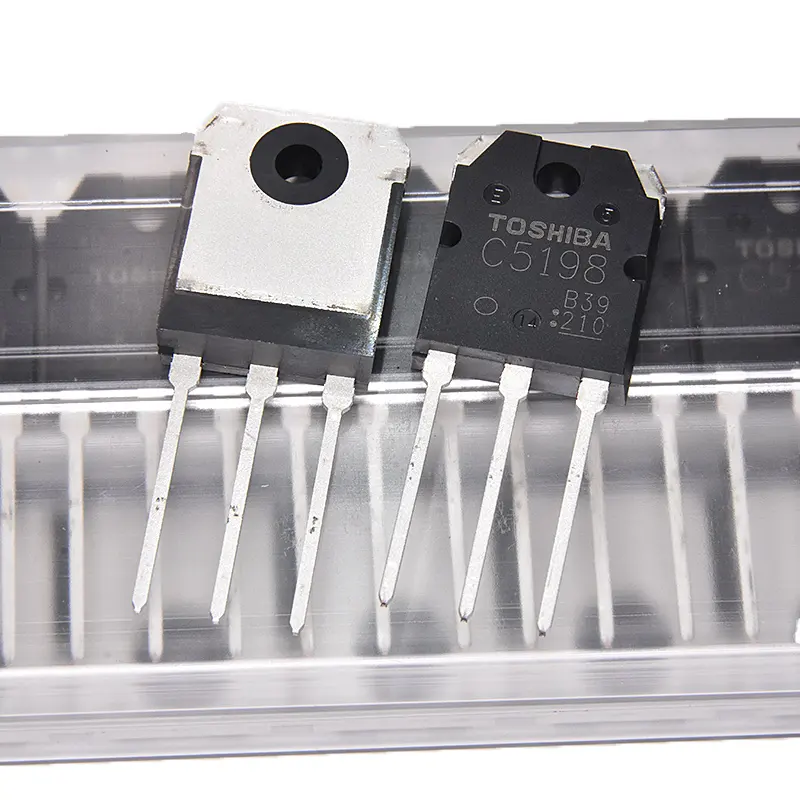
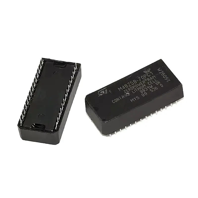
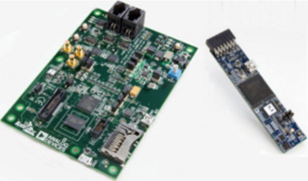
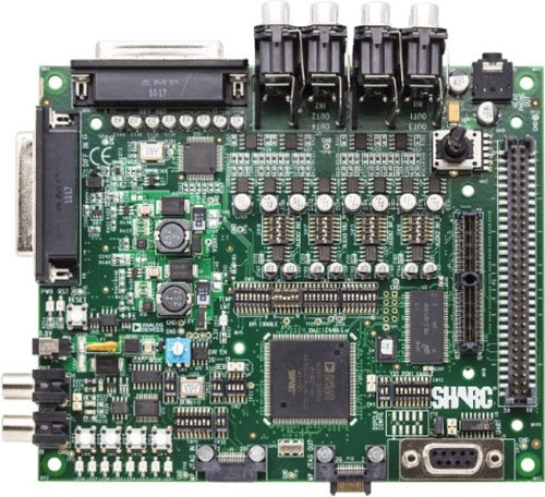
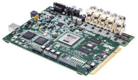
पीसीबी डिज़ाइन और निर्माण आधुनिक इलेक्ट्रॉनिक्स उत्पादन में एक महत्वपूर्ण प्रक्रिया का प्रतिनिधित्व करता है, जिसमें इलेक्ट्रॉनिक उपकरणों के लिए आधार के रूप में कार्य करने वाले प्रिंटेड सर्किट बोर्ड के निर्माण और विनिर्माण को शामिल किया जाता है। यह परिष्कृत प्रक्रिया उन्नत CAD सॉफ़्टवेयर का उपयोग करके अवधारणात्मक डिज़ाइन के साथ शुरू होती है, जहाँ इंजीनियर इलेक्ट्रॉनिक घटकों और चालक मार्गों के लेआउट की मानसिक रूप से योजना बनाते हैं। निर्माण चरण में सब्सट्रेट तैयारी, तांबा परत लगाना, फोटोरेजिस्ट लगाना, एचिंग और सतह परिष्करण जैसे कई चरण शामिल होते हैं। आधुनिक पीसीबी डिज़ाइन और निर्माण सुविधाएँ सटीक घटक स्थापना, स्वचालित परीक्षण और गुणवत्ता नियंत्रण उपायों के लिए अत्याधुनिक उपकरणों का उपयोग करती हैं। यह प्रक्रिया एकल-परत से लेकर जटिल बहु-परतीय डिज़ाइन तक विभिन्न प्रकार के बोर्ड के लिए उपयुक्त है, जो उपभोक्ता इलेक्ट्रॉनिक्स से लेकर एयरोस्पेस तकनीक तक अनुप्रयोगों का समर्थन करता है। उन्नत सुविधाओं में प्रतिबाधा नियंत्रण, तापीय प्रबंधन समाधान और उच्च-घनत्व अंतरसंबंध (HDI) क्षमताएँ शामिल हैं। उद्योग लघुकरण, उच्च प्रदर्शन और सुधारित विश्वसनीयता की मांगों को पूरा करने के लिए लगातार विकसित हो रहा है। निर्माण सुविधाएँ अंतरराष्ट्रीय मानकों के सख्ती से पालन के साथ-साथ विशिष्ट परियोजना आवश्यकताओं के लिए अनुकूलन विकल्प भी प्रदान करती हैं।