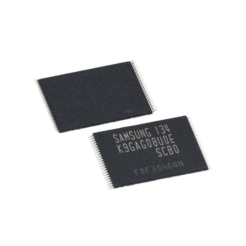
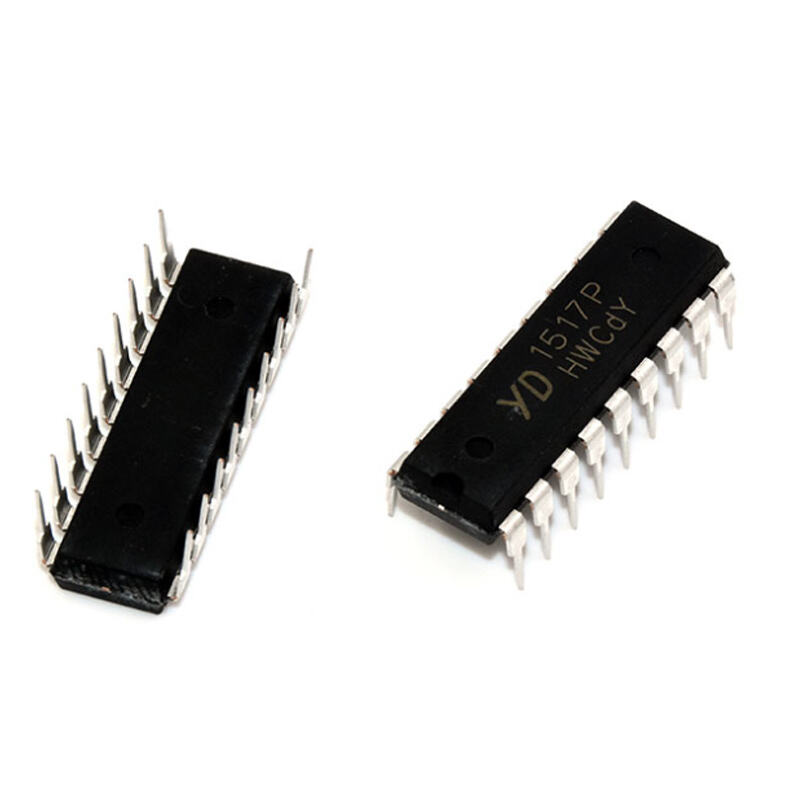
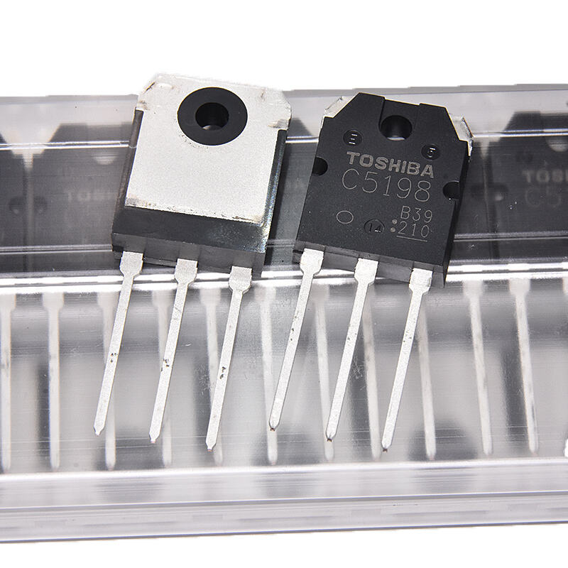
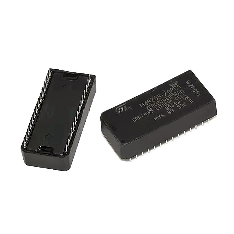
توسعه pcb
توسعه برد مدار چاپی (PCB) فرآیندی حیاتی در تولید الکترونیک مدرن محسوب میشود که شامل طراحی، نمونهسازی و تولید برد مدار چاپی است. این فرآیند پیشرفته، نرمافزارهای طراحی به کمک رایانه (CAD)، تکنیکهای تولید دقیق و رویههای آزمون سختگیرانه را برای ایجاد پایههای الکترونیکی قابل اعتماد تلفیق میکند. چرخه توسعه با ثبت شماتیک آغاز میشود، جایی که مهندسان مفاهیم مداری را به طرحهای دیجیتال تبدیل میکنند، و سپس مرحله قرارگیری قطعات و بهینهسازی مسیریابی انجام میشود. توسعه مدرن PCB از فناوریهای چندلایه بهره میبرد که امکان ایجاد مدارهای پیچیده در فضاهای کوچک را فراهم میکند و در عین حال یکپارچگی سیگنال و سازگاری الکترومغناطیسی را حفظ میکند. این فرآیند بر طراحی برای امکانپذیری تولید (DFM) تأکید دارد تا تولید مقرونبهصرفه ضمن رعایت مشخصات عملکردی تضمین شود. ویژگیهای پیشرفته شامل کنترل امپدانس، راهکارهای مدیریت حرارتی و ملاحظات طراحی با سرعت بالا است. توسعه PCB در صنایع متنوعی از الکترونیک مصرفی تا کاربردهای هوافضا استفاده میشود و خود را با الزامات خاصی همچون مدارهای انعطافپذیر برای دستگاههای تلفن همراه یا بردهای سفت برای تجهیزات صنعتی تطبیق میدهد. این فرآیند همچنین شامل مراحل تأیید جامعی است که از بررسی قوانین طراحی تا آزمون الکتریکی را در بر میگیرد و عملکرد و قابلیت اطمینان را تضمین میکند.