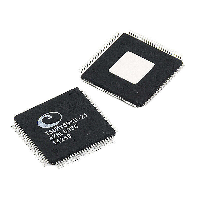
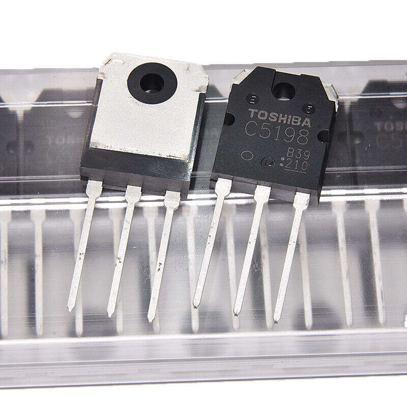
desenvolvimento de pcb
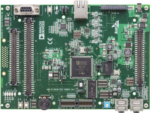
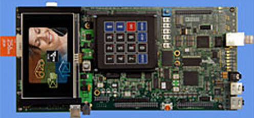
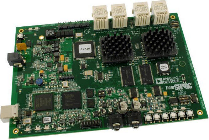
O desenvolvimento de PCB representa um processo crucial na fabricação moderna de eletrônicos, englobando o projeto, prototipagem e produção de placas de circuito impresso. Esse processo sofisticado integra softwares avançados de projeto assistido por computador (CAD), técnicas de fabricação de precisão e protocolos rigorosos de testes para criar bases eletrônicas confiáveis. O ciclo de desenvolvimento começa com a captura esquemática, onde engenheiros transformam conceitos de circuitos em projetos digitais, seguido pelo posicionamento de componentes e otimização de roteamento. O desenvolvimento moderno de PCB incorpora tecnologias de múltiplas camadas, permitindo circuitos complexos em espaços compactos, mantendo a integridade do sinal e a compatibilidade eletromagnética. O processo enfatiza o projeto para facilitar a fabricação (DFM), garantindo produção economicamente viável enquanto atende às especificações de desempenho. Recursos avançados incluem controle de impedância, soluções de gerenciamento térmico e considerações de projeto de alta velocidade. O desenvolvimento de PCB atende a diversas indústrias, desde eletrônicos de consumo até aplicações aeroespaciais, adaptando-se a requisitos específicos, como circuitos flexíveis para dispositivos móveis ou placas rígidas para equipamentos industriais. O processo também inclui etapas abrangentes de verificação, desde a verificação de regras de projeto até testes elétricos, assegurando funcionalidade e confiabilidade.